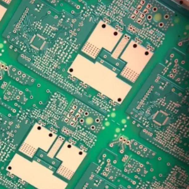
Double-Sided PCBs
At Epitome, with a unit dedicated to manufacturing double-sided PCBs, we exemplify quality, production standards and customer-centricity. Here’s more to our double-sided PCBs and its benefits.
- Robust and reliable manufacturing process.
- Same bath used to etch both sides at the same time.
- Increased surface area in the same-size-single-layer board due to the second layer of copper and vias in a double-layer board.
Details of Our Double-Sided PCBs
Here are technical features of our double-sided PCBs.
-
Type of Laminates Used
FR4, High TG FR 4, PTFE, CEM3
-
Laminate Thickness
0.4 mm to 3.2 mm
-
Base Cu Foil Thickness
18/18, 35/35, 70/70, and 105/105 µm
-
Min. Track Width/Space
4/4 Mil
-
Min. Drill Size
0.2 mm
-
Maximum PCB Size
1200mm X 630mm
-
Surface Finish
OSP, HAL (Lead Free/ Tin Lead) Immersion Tin, Electrolytic Gold Plating, ENIG
-
Other Capabilities
Carbon Key, Peelable, Via Filling, Blind and Buried Vias
Production Infrastructure Used in Double-Sided PCBs
At Epitome, we leverage the latest and the most competent infrastructure to maintain the expected and world-class quality standards for our clients, each of which is a brand.
- CNC drilling – 100 spindle capacity
- Horizontal De-Smear and direct metallization line
- Class 10K Clean Room for Photo Imaging
- Cut sheet laminator
- CCD camera assignment exposing machine
- Vertical Continuous Plater (VCP) Lines
- Vacuum etching line
- Automatic Optical Inspection (AOI), SES, DES
- Fully automatic screen printing for photo image able solder mask, class 100K clean room
- Fully automatic legend printing
- HAL (TIN lead), HAL (lead free), horizontal immersion TIN, OSP, ENIG lines , Electrolytic Gold Plating.
- Auto BBT, Universal BBT, Flying Probe Testers
- Plasma Desmear for PTFE laminates.